Three recent studies by Dr Chen and international collaborators showcase innovative approaches to material engineering. Rather than focusing solely on chemical composition, the research explores how a material’s shape, internal structure arrangement, and controlled imperfections can influence performance, addressing challenges in developing lighter, stronger, and more sustainable technologies.
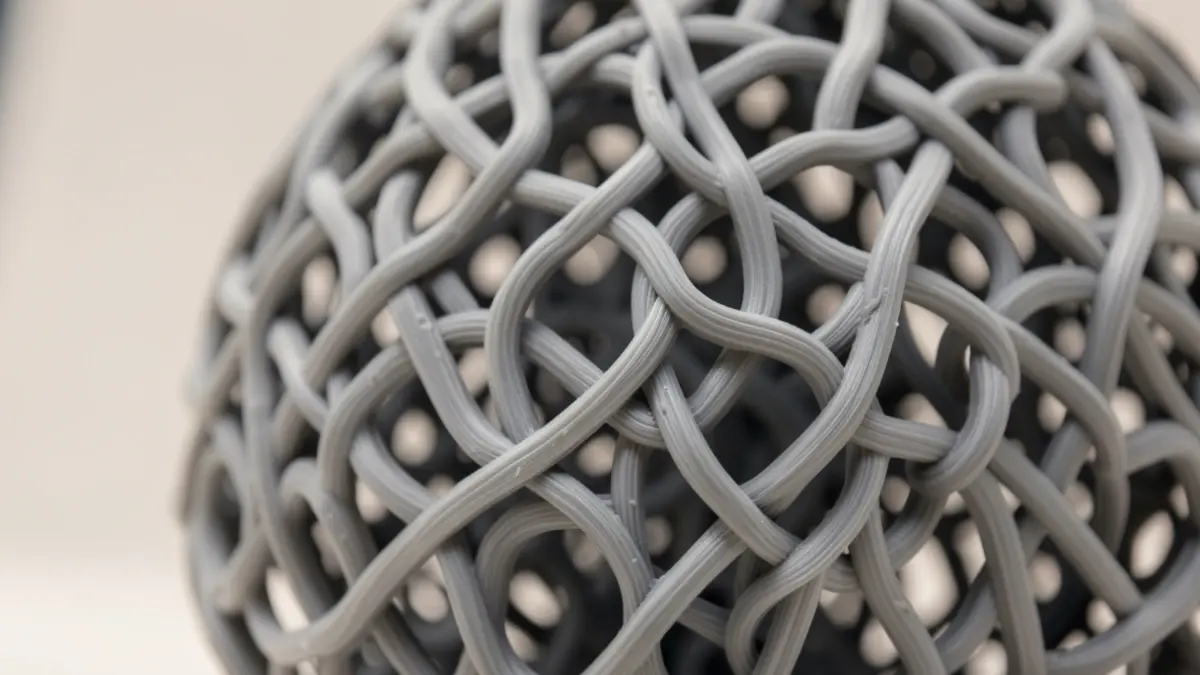
The first study, published in PNAS, introduces 'entanglement-driven responses through multiscale 3D-printed knits'. Researchers have mimicked the properties of knitted textiles in solid 3D-printed materials, creating the smallest knitted structures ever made, measuring about 50 micrometres across. These structures can stretch, deform, and recover their shape due to the interaction of interlocking loops, establishing entanglement as a new engineering design principle for tailoring mechanical behaviour.
Dr Chen explained, “This work establishes entanglement as a new engineering design principle. It allows us to tailor mechanical behaviour of materials like flexibility, resilience and adaptability through geometry and topology, not just through chemistry.” This research has implications for soft robotics, wearable technologies, medical implants, flexible electronics, and lightweight aerospace systems.
The second study, featured in Nature Communications, details a 'vibration-assisted fabrication of thin shells with spatially distributed imperfections'. This method uses sound vibrations to create controlled imperfection patterns in thin shell structures, turning potential flaws into a programmable design tool. By altering acoustic inputs, different patterns can be generated, allowing for better understanding and prediction of structural behaviour, with applications in aerospace, energy, civil engineering, and space.
“Imperfections do not have to be random. By deliberately controlling them during manufacturing, we can better understand, predict and potentially improve the behaviour of thin-shell structures,” said Dr Chen. This technique could lead to lighter and more efficient structures.
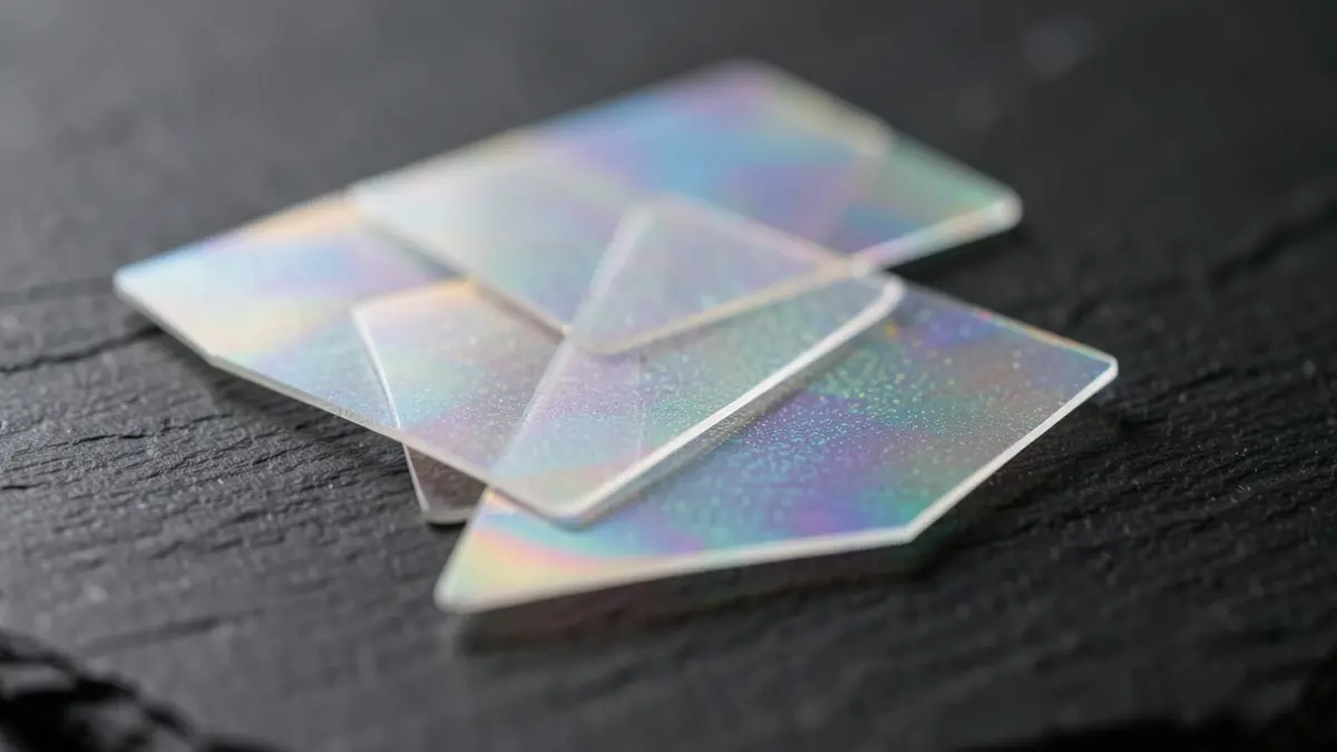
The third study, also in Nature Communications, presents 'deployable 3D architectures from wafer-fabricated precursors'. This method allows for the creation of 3D electronics from flat, 2D wafer-based manufacturing. Flat precursors are patterned and then unfold into prescribed curved geometries, creating free-standing structures without external support. This approach could enable devices to be manufactured, transported, and stored flat, then activated when needed, with potential applications in extraterrestrial habitats and deployable space systems.
Dr Chen noted, “There is growing demand for devices that conform to curved surfaces such as biological tissues and complex environments. We want to show that existing semiconductor manufacturing infrastructure can support a much broader class of devices than people currently imagine.”